From specification to GDSII: analog and mixed-signal silicon, designed and signed off
Mikroelektronix designs custom analog and mixed-signal integrated circuits: references, bias networks, comparators, current-mode arrays, low-noise amplifiers, data-converter front ends and the digital control around them. We take a block or a full chip through schematic, transistor-level verification, layout, sign-off and foundry delivery.
Our services See a delivered chip: p-ASIC Request a quote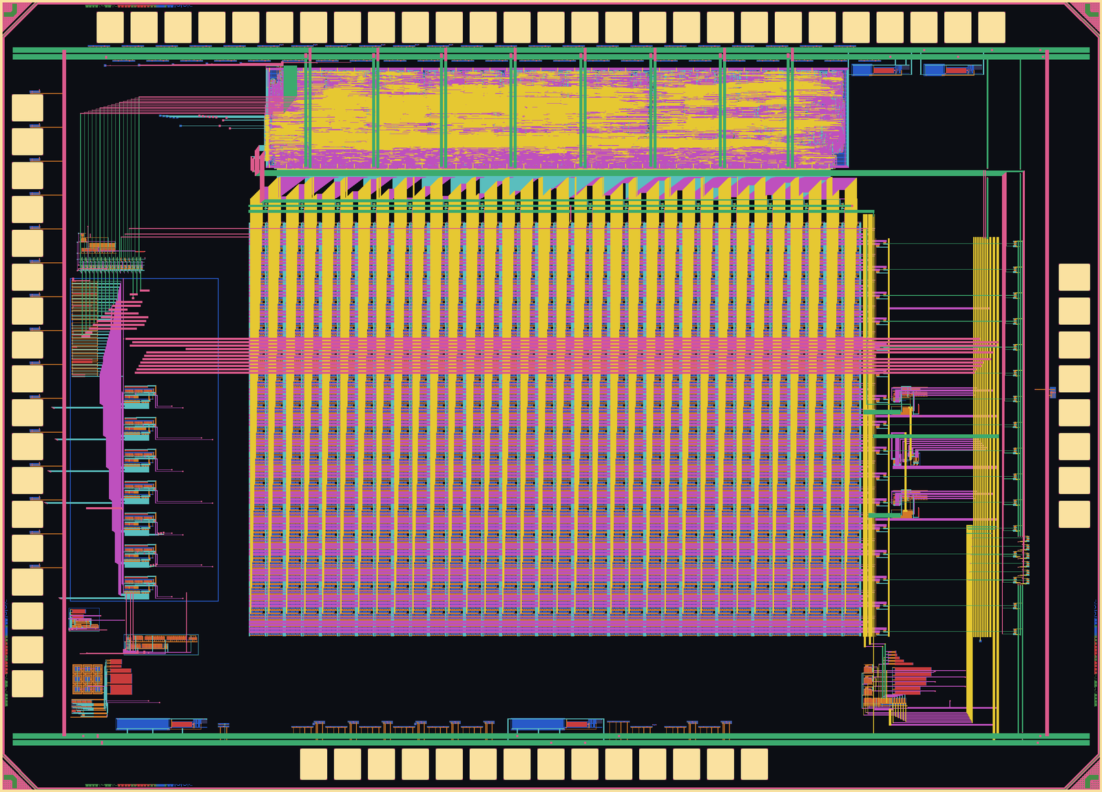
What we design for you
Custom circuits for customers who need silicon that measures, converts, references or decides. Each service is delivered with simulation reports, layout and the verification evidence.
Analog IC design
Operational and transconductance amplifiers, comparators, bandgap and current references, bias and trim networks, oscillators, level shifters and LDO regulators. Designed against your PVT corners, noise and mismatch budgets.
Mixed-signal integration
ADC / DAC front ends, sample-and-hold and sense amplifiers, current-mode compute arrays, digital calibration and trim loops, SPI / register interfaces, clocking and sequencing logic, all on one die with clean domain separation.
Physical design & layout
Matched and common-centroid analog layout, script-generated arrays, guard rings and isolation, power meshes and IR-drop-aware routing, ESD and pad rings, seal ring and dummy fill. Parasitic extraction and post-layout re-simulation included.
Verification & sign-off
Transistor-level corner, Monte-Carlo and transient-noise simulation, static timing of the digital core, DRC / LVS / ERC / antenna / density sign-off, ESD review and a documented waiver package for the foundry.
Tape-out & foundry delivery
GDSII generation, pinout and pad-label verification, delivery dossier with checksums, MPW or dedicated-run submission, packaging and bond-diagram support, and the bring-up plan for first silicon.
Test boards & characterisation
Evaluation PCBs with regulated supplies, Kelvin sensing and trim control, FPGA or MCU firmware for register access, Python measurement scripts, and characterisation reports that close the loop with the simulation models.
How a project runs
Fixed milestones, each with a review and a deliverable you can inspect.
Portfolio: a delivered chip, p-ASIC
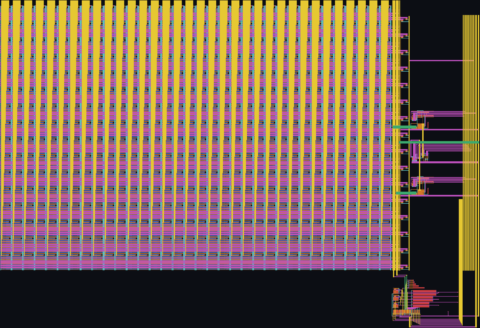
A 16-spin Probabilistic Processing Unit in 65 nm CMOS, taped out in August 2026. Every stage above is documented under the p-ASIC tab, from the circuits to the GDSII dossier.
Overview
What the chip does, in one page.
Open →Circuits
Synapse DAC, conveyors, fold, comparator, thermal-noise chain, references.
Open →Layout & sign-off
Every block rendered from GDSII; DRC, LVS, antenna, density, timing.
Open →Delivery package
GDSII databases, label layers, dossier declarations.
Open →Why customers work with us
- Evidence, not promises. Every number we report is traced to a simulation file, a sign-off report or a measurement; where a plan and the silicon differ, both are shown and dated.
- Layout that matches the circuit. Matched arrays, guard rings, star-connected supplies and Kelvin sensing are designed in from the floorplan, not patched at the end.
- The board is part of the chip. Pinout warnings, trim requirements and test access are documented for the board designer before tape-out.
- Small team, direct contact. You talk to the engineer who draws the transistors.