An integrated circuit designed for probabilistic computing
The Probabilistic Processing Unit (PPU) is a 16-spin mixed-signal chip that solves combinatorial optimisation problems compiled into QUBO / Ising form by annealing them on an analog synapse array. These pages document the chip's architecture, its physical layout, the pad labels and the GDSII deliverables.
Explore the chip Layout images GDSII deliverables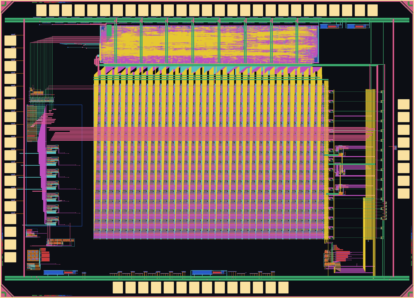
What is documented here
Every physical output produced during the tape-out of PPU Version A: layout, pad map, GDSII files, verification results and the presentations that explain the design.
PPU chip architecture
Signal path, synapse cell, thermal-noise chain, comparator, sequencer and the weight-loading path. The anatomy of one 100 ns spin decision.
Read the architecture →Layout (physical design)
Full chip, synapse bank, array tile, noise chain, bandgap, conveyor, fold / comparator and digital block, all rendered from GDSII.
See the images →Pad labels
Position, direction, supply domain and function of all 67 pads. Three critical warnings for the board designer.
Pinout table →GDSII delivery
Filled and unfilled GDSII databases, top cells, label layers, dummy-fill statistics and sign-off results.
Delivery package →Application: integer factorization
The N = 77 = 7 × 11 example compiled end to end, and a measurement of how many digits an eFlash-based ASIC could reach.
Read the example →Presentations
"PPU Version A — Explained", the noise-source and weight-loading Q&A deck and the pad-label deck, downloadable as PDF.
Go to the decks →Why a probabilistic processor?
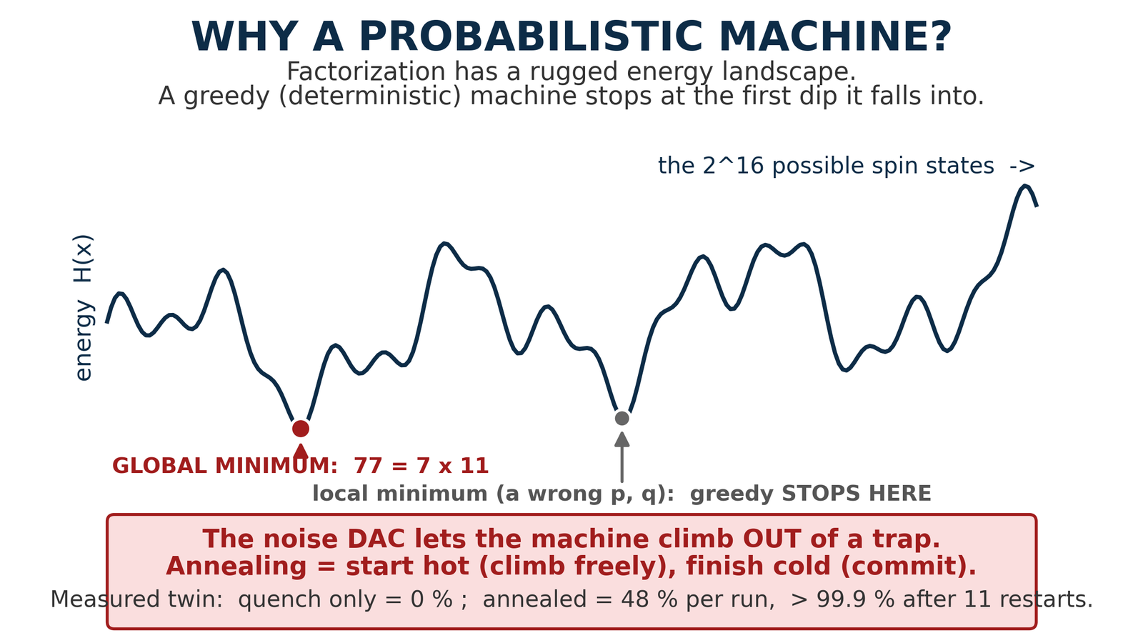
Integer factorization, MaxCut or the travelling-salesman problem have rugged energy landscapes: a deterministic (greedy) machine stops in the first valley it meets. In the PPU every spin decision is made by adding physical thermal noise to the local field that the synapse array produces as a Kirchhoff current sum. The noise amplitude is the temperature; the annealing schedule (SCHED) walks from hot to cold and a final quench freezes the answer.
Nothing in the chip is specific to a problem: the problem lives only in two small integer tables (the coupling matrix and the bias vector). The same silicon solves a different problem when the weights change.
Design philosophy: weights are written once, spins are rewritten every 100 ns, the noise value is fresh in every slot, and the noise amplitude steps down with the annealing programme.
Design flow
Five steps from a problem to silicon; only the fifth one spends time.
Steps 1–4 run on a computer (Python); the chip only ever sees 240 weight codes, 16 bias codes and a temperature schedule.