Pad labels: 67 pads, 4 supply domains, 3 warnings
Every pad carries its label in the GDSII as 6 µm text on the pin layers (M9 pin 139/0, M6 pin 136/0, M7 pin 137/0); labels were verified on 67 of 67 pads. LVS read the port names directly from these labels and returned CORRECT. The map below was drawn by reading the labels straight from the GDS.
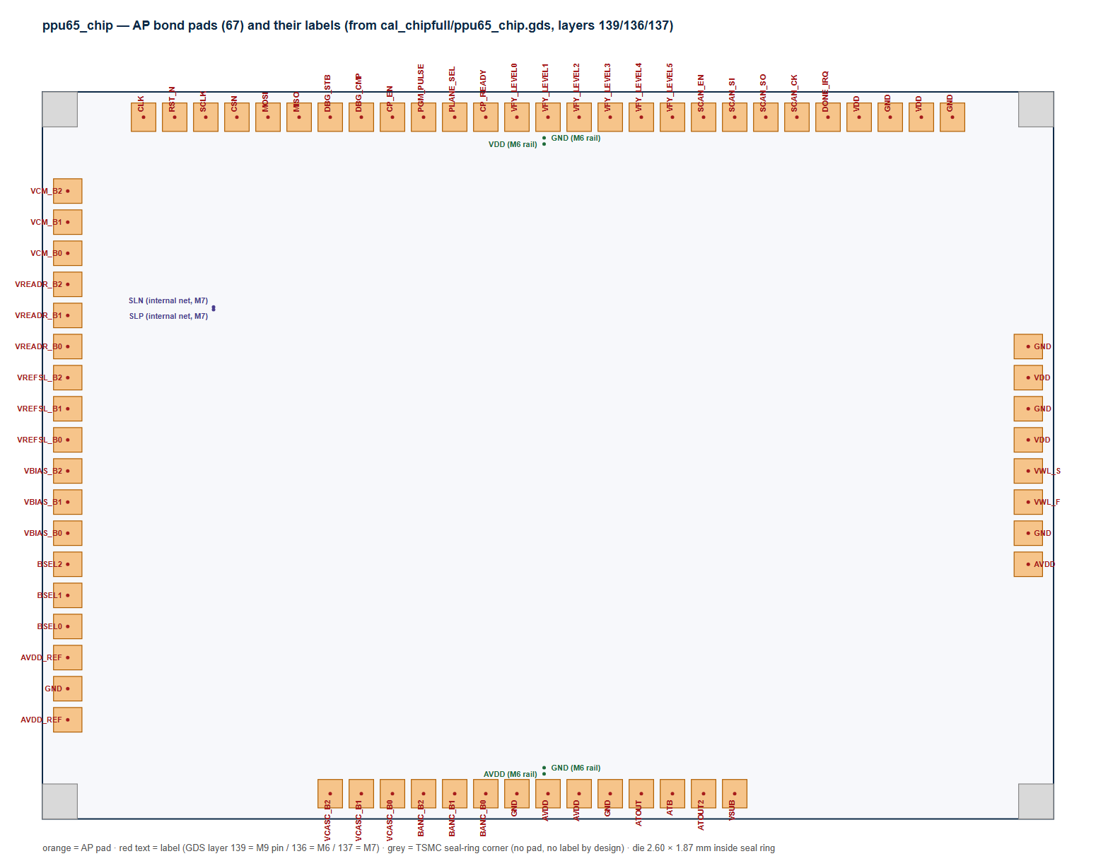
Three critical warnings for the board designer
⚠ CP_READY and VFY_LEVEL[5:0]
There is no internal pull-up. They must be driven on the board, and tied to ground if unused. The signed-off netlist contains not a single resistor.
⚠ The 18 trim bits are real chip ports
If the three bits each of VBIAS, VREFSL, VREADR, VCM, VCASC and BANC are not driven, the gates float, the trim code is undefined and the chip cannot be measured. Trims are set once per chip; BSEL once per problem.
⚠ VSUB is connected to nothing inside the chip
It has no ESD diode either. The substrate is grounded through the seal-ring P+ tap. The board must not count VSUB as a ground pad; the real GND pad count is 8.
North edge: digital and control (27 pads)
VDD domain (1.2 V). y = +1435 µm; x from CLK (−330) to GND (+1750) in 80 µm steps, left to right.
| # | Label | Type | X (µm) | Y (µm) | Function |
|---|---|---|---|---|---|
| 1 | CLK | input | -330 | +1435 | System clock of the digital core (sequencer; independent of SPI). One decision slot = 12 clock cycles. |
| 2 | RST_N | input | -250 | +1435 | Active-low asynchronous reset: sequencer state, weight latches, spin register. |
| 3 | SCLK | input | -170 | +1435 | SPI slave clock input (mode 0). |
| 4 | CSN | input | -90 | +1435 | SPI chip select (active low). |
| 5 | MOSI | input | -10 | +1435 | SPI data in: the 544 weights, the SCHED table, NSPIN and the control registers (RUN / QUENCH); CRC-16 protected. |
| 6 | MISO | output | +70 | +1435 | SPI read-back: the 16-bit spin register (the answer), status / DONE, register contents. |
| 7 | DBG_STB | output | +150 | +1435 | Debug: the comparator sample strobe itself, one pulse per slot. An external instrument samples DBG_CMP on this edge. |
| 8 | DBG_CMP | output | +230 | +1435 | Debug: the raw comparator decision latched at each strobe — the spin-decision stream before it is written to the register (randomness / autocorrelation measurement). |
| 9 | CP_EN | output | +310 | +1435 | eFlash program controller: charge-pump enable. No flash cell on this chip; the pin is exposed for the future eFlash bring-up. |
| 10 | PGM_PULSE | output | +390 | +1435 | eFlash ISPP program pulse (incremental-step pulse programming). Unused internally on Version A. |
| 11 | PLANE_SEL | output | +470 | +1435 | eFlash plane select: 0 = J+ plane, 1 = J− plane, during program / erase-verify. Unused internally on Version A. |
| 12 | CP_READY | input | +550 | +1435 | Charge-pump ready handshake. ⚠ No internal pull-up: must be driven on the board (tie low if unused). |
| 13 | VFY_LEVEL0 | input | +630 | +1435 | 6-bit verify level (read-back Vt for the ISPP loop), bit 0. ⚠ No internal pull-up: must be driven on the board. |
| 14 | VFY_LEVEL1 | input | +710 | +1435 | Verify level bit 1. ⚠ No internal pull-up. |
| 15 | VFY_LEVEL2 | input | +790 | +1435 | Verify level bit 2. ⚠ No internal pull-up. |
| 16 | VFY_LEVEL3 | input | +870 | +1435 | Verify level bit 3. ⚠ No internal pull-up. |
| 17 | VFY_LEVEL4 | input | +950 | +1435 | Verify level bit 4. ⚠ No internal pull-up. |
| 18 | VFY_LEVEL5 | input | +1030 | +1435 | Verify level bit 5 (MSB). ⚠ No internal pull-up. |
| 19 | SCAN_EN | reserved / NC | +1110 | +1435 | Reserved / not connected: the digital core has no scan chain. Pad kept for pin compatibility with a later revision. |
| 20 | SCAN_SI | reserved / NC | +1190 | +1435 | Reserved / not connected (scan-chain input). |
| 21 | SCAN_SO | reserved / NC | +1270 | +1435 | Reserved / not connected (scan-chain output). |
| 22 | SCAN_CK | reserved / NC | +1350 | +1435 | Reserved / not connected (scan clock). |
| 23 | DONE_IRQ | reserved / NC | +1430 | +1435 | Reserved / not connected: on Version A, DONE is read through the SPI status register. |
| 24 | VDD | supply | +1510 | +1435 | 1.2 V digital supply (SPI, register file, sequencer, weight latches, spin register). RC-triggered power clamp. |
| 25 | GND | ground | +1590 | +1435 | Common ground (a single net for digital and analog; separation is done on the board). Eight real GND pads in total. |
| 26 | VDD | supply | +1670 | +1435 | 1.2 V digital supply (SPI, register file, sequencer, weight latches, spin register). RC-triggered power clamp. |
| 27 | GND | ground | +1750 | +1435 | Common ground (a single net for digital and analog; separation is done on the board). Eight real GND pads in total. |
East edge: supplies and the word-line voltage (8 pads)
x = +1945 µm; y from 285 to 845.
| # | Label | Type | X (µm) | Y (µm) | Function |
|---|---|---|---|---|---|
| 1 | AVDD | supply | +1945 | +285 | 2.5 V analog supply: synapse array, conveyors, fold, StrongARM comparator, noise chain, level shifters. Power clamp (3000 µm). |
| 2 | GND | ground | +1945 | +365 | Common ground (a single net for digital and analog; separation is done on the board). Eight real GND pads in total. |
| 3 | VWL_F | supply | +1945 | +445 | 1.0 V word-line supply, FORCE side: powers the WL drivers; WL high = 1.0 V is the spin '1' level seen by the synapse switches. |
| 4 | VWL_S | analog | +1945 | +525 | Kelvin SENSE of the same word-line supply: carries no current; joins VWL_F at the board's star point so the regulator sees the on-chip voltage. |
| 5 | VDD | supply | +1945 | +605 | 1.2 V digital supply (SPI, register file, sequencer, weight latches, spin register). RC-triggered power clamp. |
| 6 | GND | ground | +1945 | +685 | Common ground (a single net for digital and analog; separation is done on the board). Eight real GND pads in total. |
| 7 | VDD | supply | +1945 | +765 | 1.2 V digital supply (SPI, register file, sequencer, weight latches, spin register). RC-triggered power clamp. |
| 8 | GND | ground | +1945 | +845 | Common ground (a single net for digital and analog; separation is done on the board). Eight real GND pads in total. |
South edge: trims, supplies and analog test (14 pads)
y = −305 µm; x from 150 to 1190.
| # | Label | Type | X (µm) | Y (µm) | Function |
|---|---|---|---|---|---|
| 1 | VCASC_B2 | trim bit | +150 | -305 | VCASC trim (MSB): cascode bias of the fold's current mirror. ⚠ Must be driven on the board. |
| 2 | VCASC_B1 | trim bit | +230 | -305 | VCASC trim bit 1. ⚠ Must be driven on the board. |
| 3 | VCASC_B0 | trim bit | +310 | -305 | VCASC trim bit 0. ⚠ Must be driven on the board. |
| 4 | BANC_B2 | trim bit | +390 | -305 | BANC trim (MSB): the fold's fixed anchor, the per-chip comparator-offset trim (nominal code 3). ⚠ Must be driven on the board. |
| 5 | BANC_B1 | trim bit | +470 | -305 | BANC trim bit 1. ⚠ Must be driven on the board. |
| 6 | BANC_B0 | trim bit | +550 | -305 | BANC trim bit 0. ⚠ Must be driven on the board. |
| 7 | GND | ground | +630 | -305 | Common ground (a single net for digital and analog; separation is done on the board). Eight real GND pads in total. |
| 8 | AVDD | supply | +710 | -305 | 2.5 V analog supply: synapse array, conveyors, fold, StrongARM comparator, noise chain, level shifters. Power clamp (3000 µm). |
| 9 | AVDD | supply | +790 | -305 | 2.5 V analog supply: synapse array, conveyors, fold, StrongARM comparator, noise chain, level shifters. Power clamp (3000 µm). |
| 10 | GND | ground | +870 | -305 | Common ground (a single net for digital and analog; separation is done on the board). Eight real GND pads in total. |
| 11 | ATOUT | analog | +950 | -305 | Analog test-mux OUTPUT: 16 internal nodes (SLP, SLN, BSENSE, bias rails …) selected one-hot by an SPI register → 16 switches → buffer → pad. |
| 12 | ATB | analog | +1030 | -305 | Analog Test Bus: the raw node where the 16 test switches meet, before the buffer; direct (unbuffered) access to the selected node. |
| 13 | ATOUT2 | reserved / NC | +1110 | -305 | Reserved / not connected (second test output, unused on Version A). |
| 14 | VSUB | reserved / NC | +1190 | -305 | ⚠ NOT CONNECTED inside the chip (LVS: the only pass-through net, zero devices) and no ESD diode. The substrate is grounded through the seal ring. The board must NOT count it as a ground pad. |
West edge: reference supply and trim bits (18 pads)
AVDD_REF domain (2.5 V). x = −525 µm; y from −115 to +1245.
| # | Label | Type | X (µm) | Y (µm) | Function |
|---|---|---|---|---|---|
| 1 | AVDD_REF | supply | -525 | -115 | 2.5 V supply of the reference block: bandgap (0.927 V) → master bias (10 µA) → resistor-string taps → buffers. Bridged to AVDD by anti-parallel ESD diodes. |
| 2 | GND | ground | -525 | -35 | Common ground (a single net for digital and analog; separation is done on the board). Eight real GND pads in total. |
| 3 | AVDD_REF | supply | -525 | +45 | 2.5 V supply of the reference block: bandgap (0.927 V) → master bias (10 µA) → resistor-string taps → buffers. Bridged to AVDD by anti-parallel ESD diodes. |
| 4 | BSEL0 | input | -525 | +125 | BREF tap select bit 0: one of 8 taps for the comparator reference (0.5927 → 0.6345 V, ≈ 6 mV/step). Set PER PROBLEM. |
| 5 | BSEL1 | input | -525 | +205 | BREF tap select bit 1. |
| 6 | BSEL2 | input | -525 | +285 | BREF tap select bit 2 (MSB). |
| 7 | VBIAS_B0 | trim bit | -525 | +365 | VBIAS trim bit 0: gate of every synapse current source (0.5394 V nominal); the size of one weight unit (the α knob). ⚠ Must be driven on the board. |
| 8 | VBIAS_B1 | trim bit | -525 | +445 | VBIAS trim bit 1. ⚠ Must be driven on the board. |
| 9 | VBIAS_B2 | trim bit | -525 | +525 | VBIAS trim bit 2 (MSB). ⚠ Must be driven on the board. |
| 10 | VREFSL_B0 | trim bit | -525 | +605 | VREF_SL trim bit 0: the level the conveyors hold both source lines at (0.150 V); keeps the array summation linear. ⚠ Must be driven on the board. |
| 11 | VREFSL_B1 | trim bit | -525 | +685 | VREF_SL trim bit 1. ⚠ Must be driven on the board. |
| 12 | VREFSL_B2 | trim bit | -525 | +765 | VREF_SL trim bit 2 (MSB). ⚠ Must be driven on the board. |
| 13 | VREADR_B0 | trim bit | -525 | +845 | V_READ trim bit 0: the bit-line voltage of the selected row (0.499 V). ⚠ Must be driven on the board. |
| 14 | VREADR_B1 | trim bit | -525 | +925 | V_READ trim bit 1. ⚠ Must be driven on the board. |
| 15 | VREADR_B2 | trim bit | -525 | +1005 | V_READ trim bit 2 (MSB). ⚠ Must be driven on the board. |
| 16 | VCM_B0 | trim bit | -525 | +1085 | VCM trim bit 0: input common mode of the thermal-noise chain (0.8975 V). ⚠ Must be driven on the board. |
| 17 | VCM_B1 | trim bit | -525 | +1165 | VCM trim bit 1. ⚠ Must be driven on the board. |
| 18 | VCM_B2 | trim bit | -525 | +1245 | VCM trim bit 2 (MSB). ⚠ Must be driven on the board. |
Trim and reference groups
| Group | Bits / edge | What it sets | Nominal | When |
|---|---|---|---|---|
| BSEL[2:0] | 3 / west | One of 8 taps for the comparator reference BREF (0.5927 → 0.6345 V, ≈ 6 mV/step). The compiler picks the tap that centres the decision threshold. | per problem | every problem |
| VBIAS_B[2:0] | 3 / west | Gate voltage of every synapse current source; the size of one weight unit (≈ 6.7–7.4 µA): the array's α knob. | 0.5394 V | per chip |
| VREFSL_B[2:0] | 3 / west | The level the conveyors hold both source lines at; keeps the array sum linear (35 % compression without it). | 0.150 V | per chip |
| VREADR_B[2:0] | 3 / west | The voltage the bit line of the selected row is driven to. | 0.499 V | per chip |
| VCM_B[2:0] | 3 / west | Input common mode of the thermal-noise chain (A1 gates). | 0.8975 V (target 0.900) | per chip |
| VCASC_B[2:0] | 3 / south | Cascode bias of the fold's current mirror; mirror output impedance / copy accuracy (2.49 mV/step). | ≈ 0.75 V | per chip |
| BANC_B[2:0] | 3 / south | The fold's fixed anchor; the per-chip comparator-offset trim knob (2.58 mV/step, 18 mV range, nominal code 3). | 0.620 V | per chip |
Reference chain: bandgap (0.927 V) → master bias (10 µA seed) → resistor-string taps → buffers. AVDD_REF is bridged to AVDD by anti-parallel ESD diodes.
ESD protection
- Dual diodes on all 48 signal pads: pad → GND (n-diode) and pad → the edge's supply (p-diode).
- RC-triggered power clamps on the four supply nets: VDD (2400 µm, hvt nMOS), AVDD (3000 µm, 2.5 V nMOS), AVDD_REF, VWL.
- Anti-parallel diode bridge between AVDD and AVDD_REF.
- A single ground net (digital/analog separation on the board); substrate grounded through the seal-ring P+ tap.
- The VSUB pad has no ESD diode and is unconnected (the chip's only pass-through net in LVS).
Supply domains
| Net | Voltage | Pads | Powers |
|---|---|---|---|
| VDD | 1.2 V | 4 (N2, E2) | SPI, register file, sequencer, weight latches, spin register |
| AVDD | 2.5 V | 3 (E1, S2) | Synapse array, conveyors, fold, StrongARM, noise chain, level shifters |
| AVDD_REF | 2.5 V | 2 (W) | Bandgap, master bias, resistor string, buffers |
| VWL_F / VWL_S | 1.0 V | 1 + 1 (E) | Word-line drivers (F = force, S = Kelvin sense; joined at the board's star point) |
| GND | 0 V | 8 (N2, E3, S2, W1) | Common ground |