Chip architecture: the anatomy of one spin decision
The PPU is a 16-spin Ising / QUBO solver. Weights map to currents, spins to word lines, the local field to the current difference of two source lines, and temperature to the amplitude of physical thermal noise. The signal path is explained block by block below.
At a glance
| Item | Value |
|---|---|
| Technology | 65 nm CMOS, 9 metal layers, wire-bond packaging |
| Die | 2.847 × 2.051 mm including the seal ring (5.84 mm²); 2.60 × 1.87 mm inside the seal ring |
| Problem class | QUBO / Ising — no problem-specific hardware; the problem lives only in the weights |
| Array | 16 spins × 17 columns (16 couplings + 1 bias) × 2 planes (SL+, SL−) = 544 synapse cells |
| Weight | 6-bit code in a latch per cell; six binary-weighted current legs (1:2:4:8:16:32); 3 264 latch bits |
| Unit current | ≈ 7.4 µA per weight unit (post-layout); α = 9.347 µA per QUBO unit (N = 77 example) |
| Noise source | A transistor pair's own thermal noise → 3 gain stages (≈ 1340×) → 6-bit constant-sum steerer |
| Decision | Conveyor → fold → StrongARM comparator; one decision per slot, 12 clock cycles |
| Digital core | SPI slave (mode 0, CRC-16), register file, sequencer (SCHED table, token ring), 16-bit spin register |
| Supply domains | VDD 1.2 V (digital) · AVDD 2.5 V (array and analog) · AVDD_REF 2.5 V (references) · VWL 1.0 V (word lines) |
| Pads | 67 (27 north, 8 east, 14 south, 18 west); dual ESD diodes on all 48 signal pads |
| Test access | 16-channel analog test mux (ATOUT / ATB) + SPI read-back; no scan chain |
Signal path: a problem goes in once, one spin comes out per slot
Read left to right: the weights are written before the run, currents are compared, one spin bit is produced per slot and fed straight back to the input (word line) of the next decision.
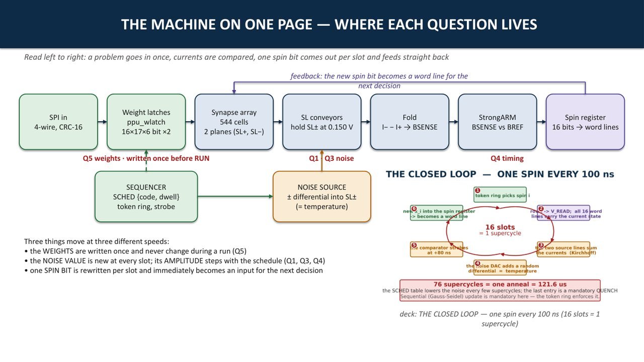
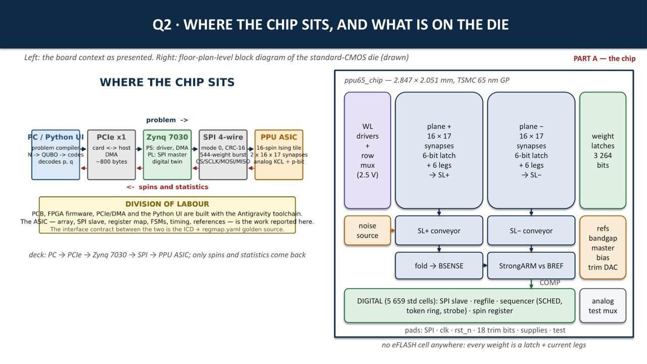
Three things, three speeds: the weights never change during a run; the noise value is new in every slot while its amplitude steps down with the schedule; one spin bit is rewritten per slot and immediately becomes an input of the next decision (Gauss–Seidel update).
Synapse cell: weight = current
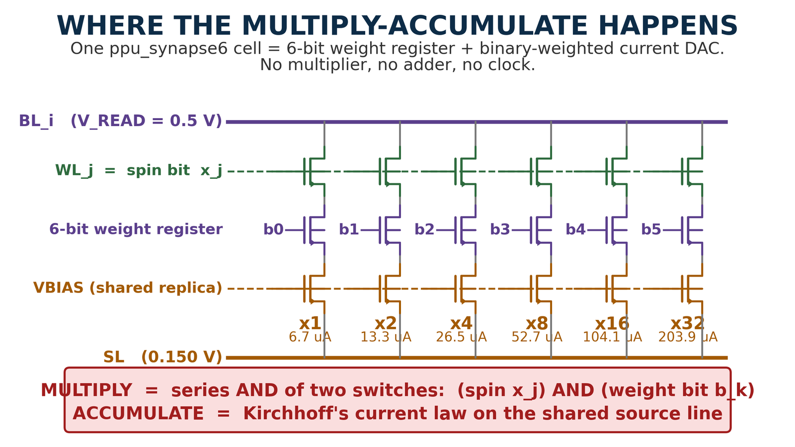
Each cell has 18 transistors: six legs, each with a spin switch (word line WL), a weight-bit switch (bk from the latch) and a current source set by VBIAS. The legs are sized ×1 … ×32; which legs are on is the weight.
- Multiply is two switches in series: (spin xj) AND (weight bit bk).
- Accumulate is Kirchhoff's current law: all cells of a row pour into the same source line (SL). No multiplier, no adder, no clock.
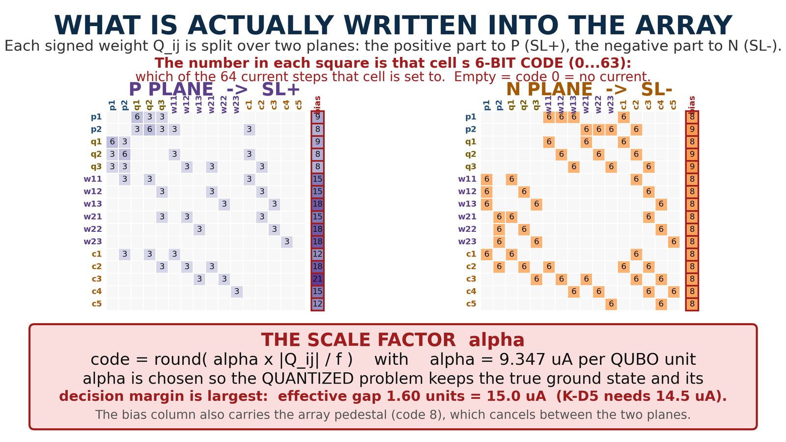
- Signed weights come from two planes: the positive part is written into the SL+ plane, the negative part into SL−. Column 17 carries the bias (a code-8 pedestal on both planes, cancelled by the difference).
- Row-current budget 400 µA per plane; worst row of the N = 77 example 351 µA.
Thermal-noise chain: the physical counterpart of temperature
In the first presentation the noise source was six current legs steered by an LFSR (linear feedback shift register). That source was abandoned the same day: an LFSR is deterministic and periodic, and its 10.2 µA full scale was below the ≥ 40 µA that factorization needs. In the manufactured chip, entropy comes from the Johnson–Nyquist noise of a transistor pair.
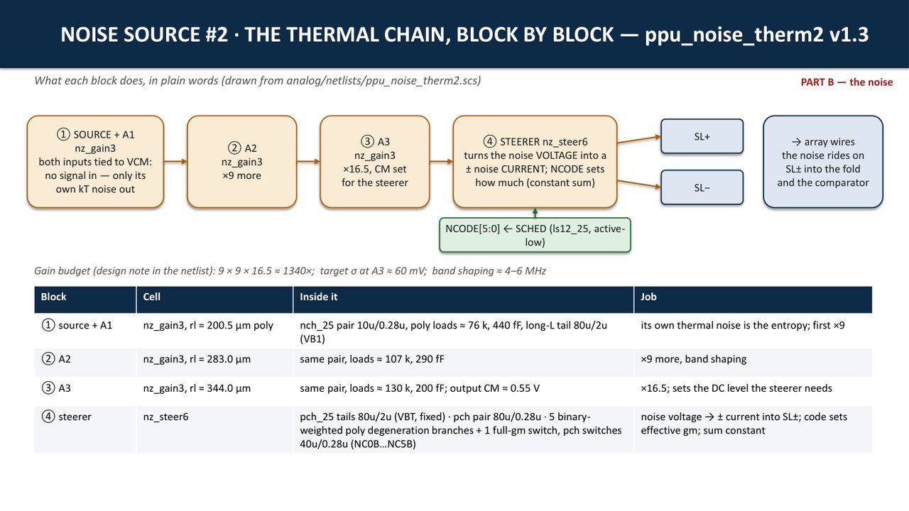
The chain, block by block (ppu_noise_therm2 v1.3)
| Block | What it does |
|---|---|
| ① Source + A1 (nz_gain3) | Both inputs of the differential pair tied to VCM: no signal, only its own thermal noise; first ×9. |
| ② A2 (nz_gain3) | ×9 more; band shaping (≈ 4–6 MHz). |
| ③ A3 (nz_gain3) | ×16.5; sets the output common mode (≈ 0.55 V) the steerer needs. |
| ④ Steerer (nz_steer6) | Turns the noise voltage into a ± current; the 6-bit NCODE sets the effective gm; the total current is constant. |
Gain budget 9 × 9 × 16.5 ≈ 1340×; target σ at the A3 output ≈ 60 mV. The loads are poly resistors, so the DC levels track the master-bias current.
Constant-sum rule: the noise moves current between SL+ and SL−, it never adds current to them. The common mode is therefore code-independent (measured: BSENSE DC 0.656 V at every code); only the difference is randomised. That is a temperature, not an offset.
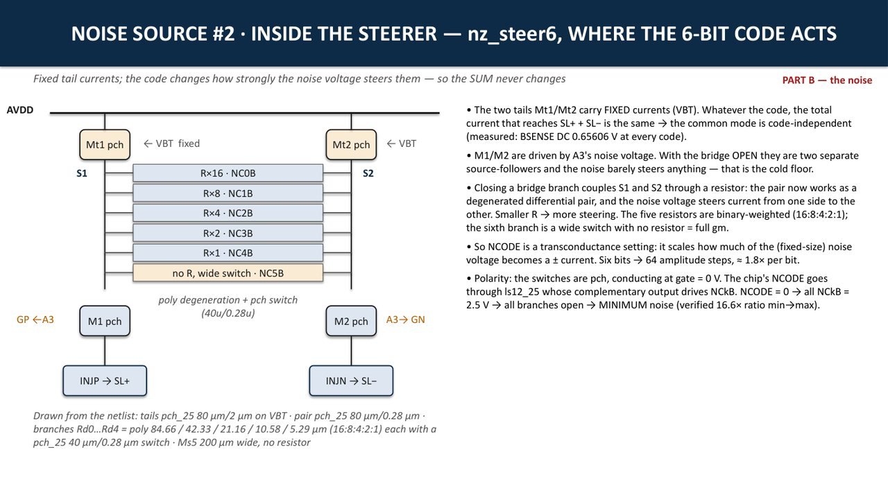
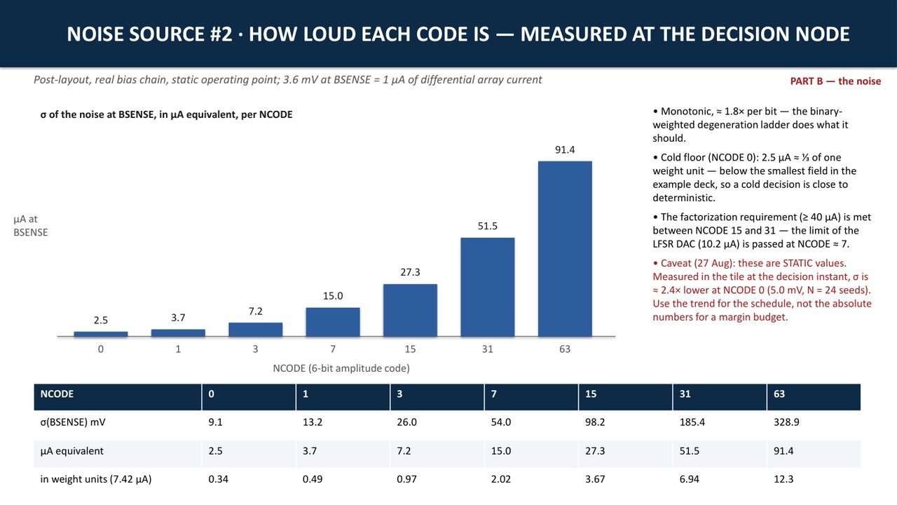
Noise amplitude per code (at the decision node, post-layout)
| NCODE | 0 | 1 | 3 | 7 | 15 | 31 | 63 |
|---|---|---|---|---|---|---|---|
| σ(BSENSE), mV | 9.1 | 13.2 | 26.0 | 54.0 | 98.2 | 185.4 | 328.9 |
| µA equivalent | 2.5 | 3.7 | 7.2 | 15.0 | 27.3 | 51.5 | 91.4 |
| in weight units (7.42 µA) | 0.34 | 0.49 | 0.97 | 2.02 | 3.67 | 6.94 | 12.3 |
Monotonic, ≈ 1.8× per bit. The cold floor (NCODE 0) is one third of a weight unit: a cold decision is close to deterministic. The ≥ 40 µA that factorization needs is passed between NCODE 15 and 31. These are static operating-point values; measured in the tile at the decision instant, σ at NCODE 0 is ≈ 2.4× lower.
Decision chain: two currents, one comparison
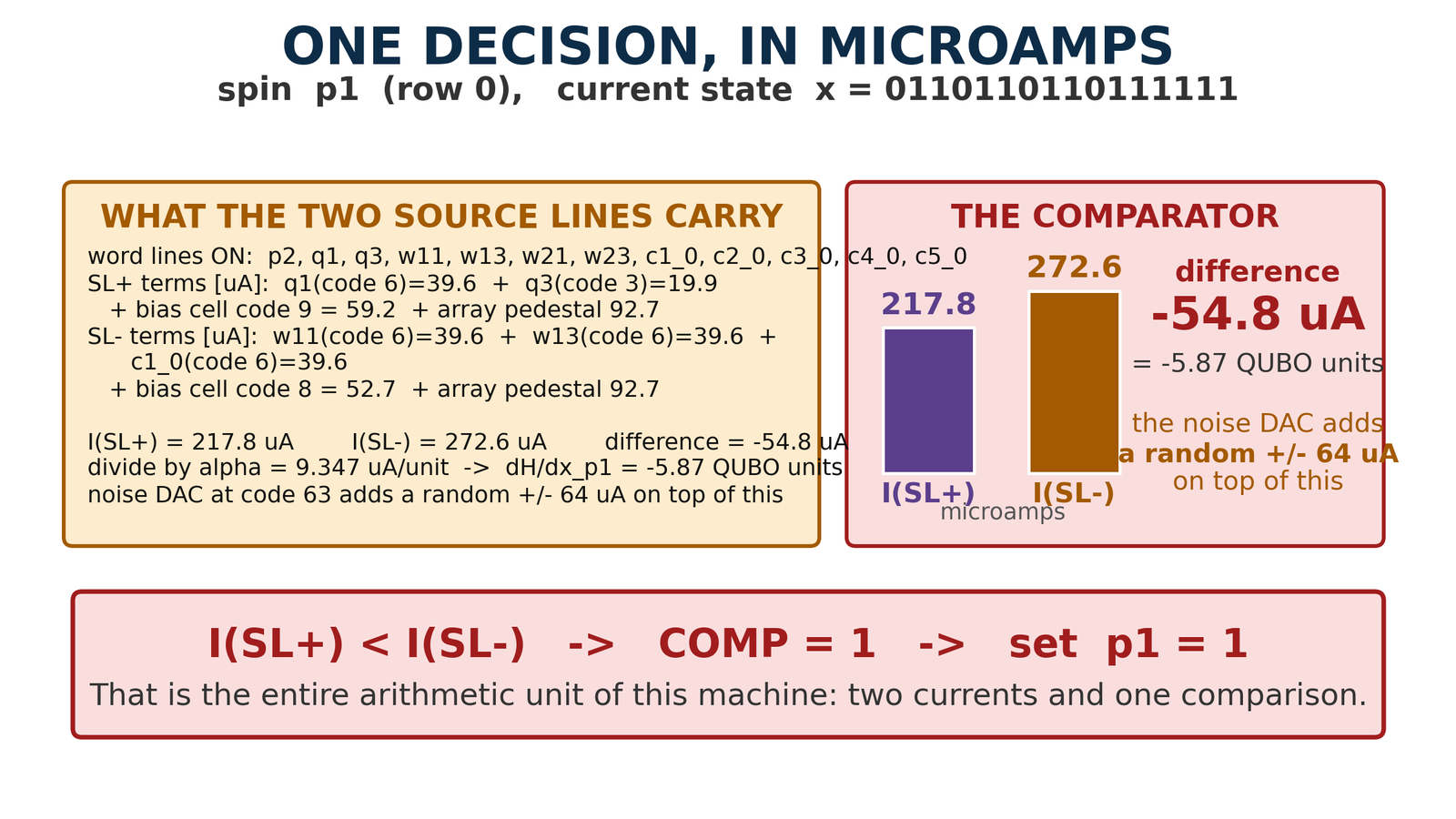
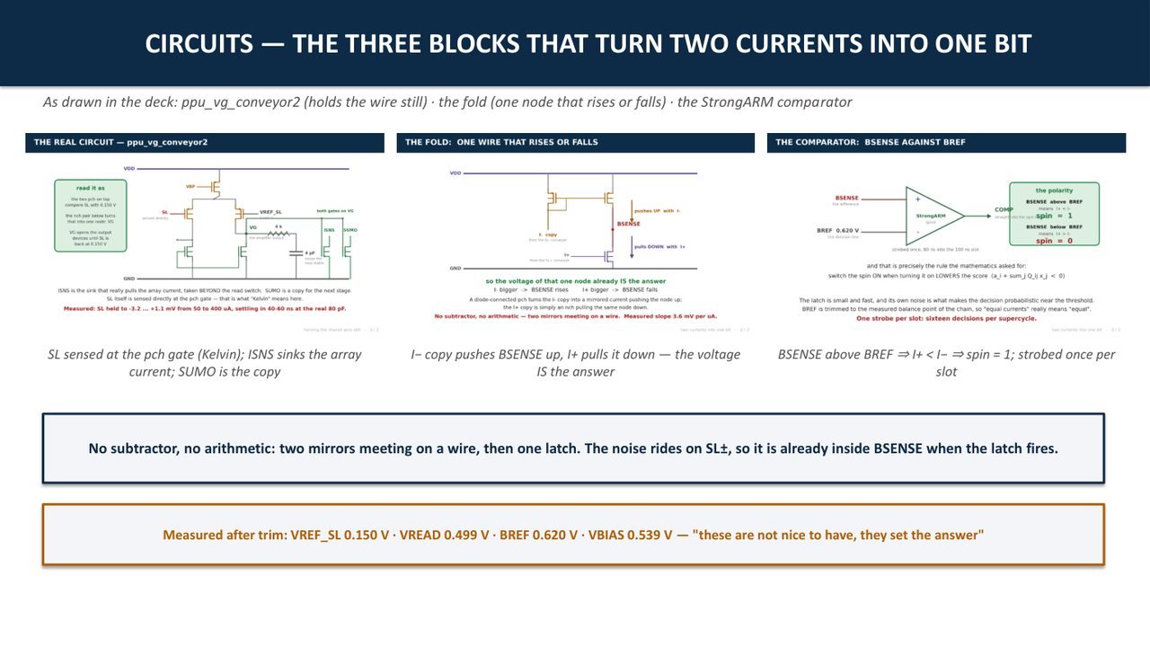
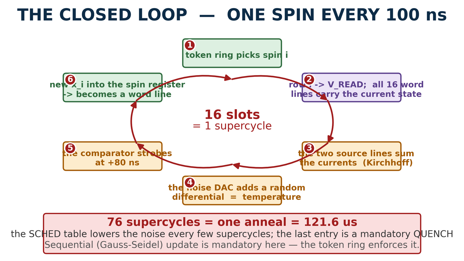
When row i is selected its bit line is driven to V_READ (0.499 V) and the 16 word lines carry the current spin state. SL+ sums the positive weights and SL− the negative ones as currents. Two conveyors hold these lines at 0.150 V and copy the currents; the fold pushes the I− node up and pulls I+ down, and the difference becomes the BSENSE voltage (3.6 mV/µA). The StrongARM comparator compares BSENSE with BREF (0.620 V, trimmed) once per slot; the result becomes bit i of the spin register.
- Without the conveyors the array sum would compress by 35 %; the VREF_SL trim keeps it linear.
- BREF is chosen per problem from an eight-tap resistor string with BSEL[2:0]; BANC is the problem-independent, per-chip offset trim.
- Decision-margin example (N = 77): 1.60 QUBO units = 15.0 µA; 14.5 µA required.
Timing and the annealing programme
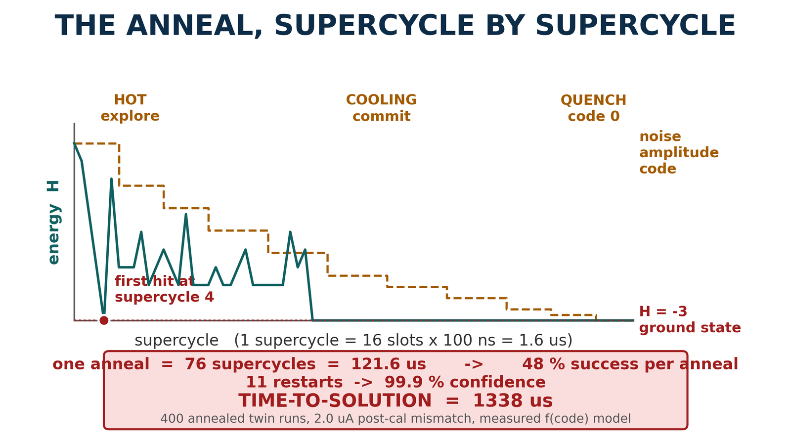
One slot = one spin decision = 12 clock cycles. 16 slots = one supercycle (every spin once). The sequencer applies the {noise code, dwell} pairs of the SCHED table in order.
| What changes? | When? |
|---|---|
| The random value of the noise | every slot — a physical process is fresh at every strobe |
| Noise amplitude (temperature, NCODE) | at every SCHED entry; constant for dwell supercycles |
| Spin bit | one bit per slot; immediately becomes the word line of the next decision |
| Weights | never during a run |
The last SCHED entry is mandatorily code 0 (quench): the machine freezes its answer. In the N = 77 example the anneal is 76 supercycles = 121.6 µs; 48 % success per anneal; time to solution 1338 µs.
A measured subtlety: at the hottest codes the noise time constant rises to ≈ 80 ns, so in a 120 ns slot neighbouring decisions share 19–23 % of a push. At cold and mid codes the decisions are independent (2–3 %). Open item for the next revision.
Where the weights come from and where they stay
The weights are loaded once before the run and never touched during the anneal; only the 16 spin bits change.
- Write protocol: row/column address plus the 6-bit codes of both planes for couplings; index plus 12 bits for biases.
- Read-back is the 16-bit spin register only; Python decodes p and q.
- The same silicon solves any problem: only the two 16 × 17 tables differ.
p-bit behaviour: a sigmoid when hot, a step when cold
Measured on a single-row chain (synapse → conveyors → fold → StrongARM) with transistor-level transient-noise analysis, 180 decisions per point:
- Hot (tail current 40 µA): a smooth sigmoid; a local field of +2.5 µA gives "1" 44 % of the time, +4 µA 86 %. The Boltzmann-like acceptance an annealer needs.
- Cold (2 µA): a hard threshold; every decision follows the sign of the field. The deterministic floor that freezes the answer.
- The centre offset (+2.8 µA) comes from the copy-path residue; the BREF trim absorbs it.
- Hot/cold ratio ≈ 36× in the v1.3 chain (2.5 → 91 µA).
After Version A
Version A (manufactured)
Standard CMOS, 65 nm. Weights in latches, entropy from a separate thermal-noise block. Purpose: prove the annealer architecture with measured device models before the eFlash weight cell exists.
Version B (spec draft)
Same signal path; noise full scale ≥ 40 µA, 64-spin target, automatic per-problem BREF calibration, a formal register map and the α band rule in the compiler.
P-FLASH (eFlash based)
55 nm embedded-Flash process: weights held as persistent multi-level eFlash threshold voltages, programmed once per problem and read billions of times. Weight traffic (the von Neumann bottleneck) disappears entirely. TÜBİTAK–JSPS bilateral project framework.