Layout: placement images rendered from GDSII
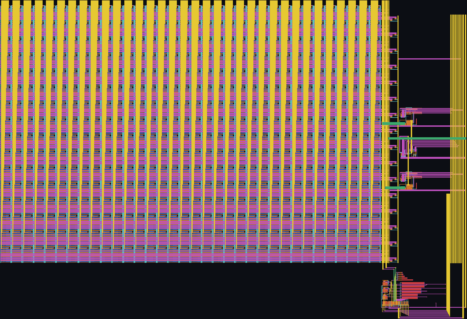
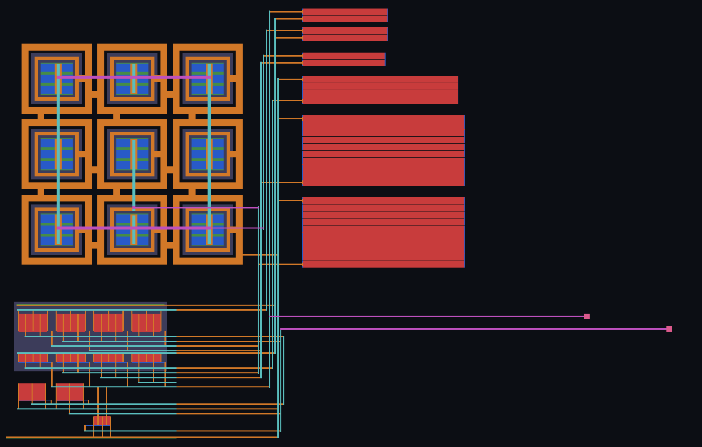
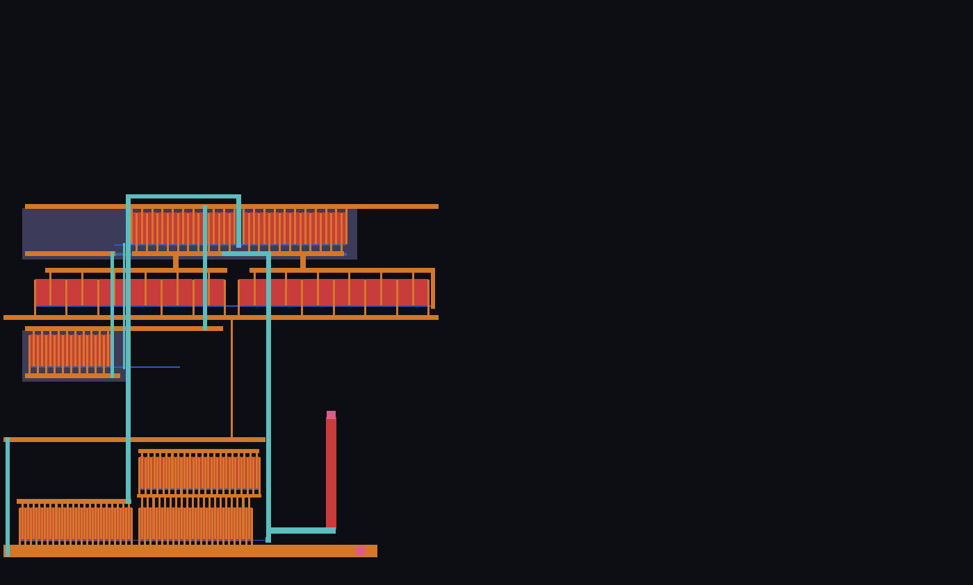
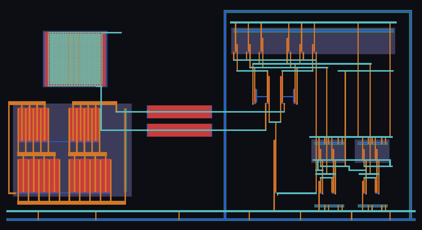
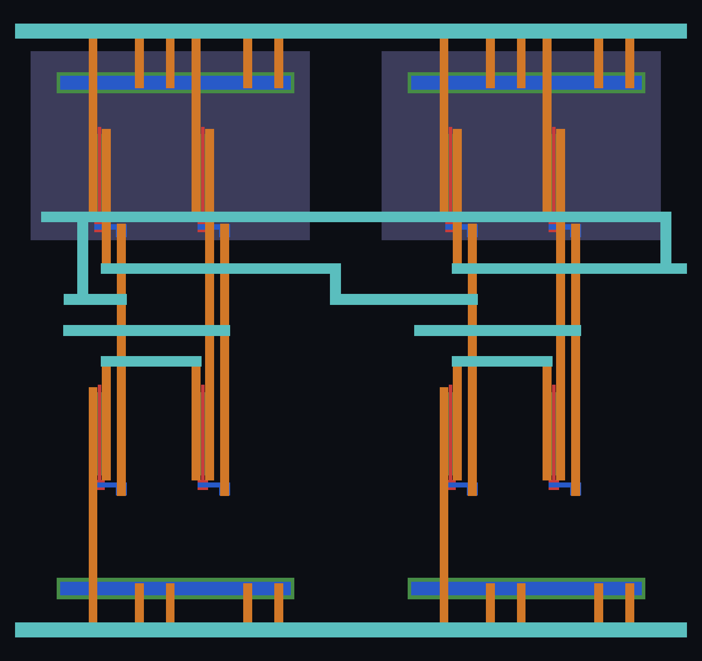
Every image below was rasterized layer by layer from the delivered GDSII database itself (ppu65_chip.gds and the block GDS files); none of them is a drawing or a schematic. The dummy-fill layers are switched off in the images.
Full chip: ppu65_chip
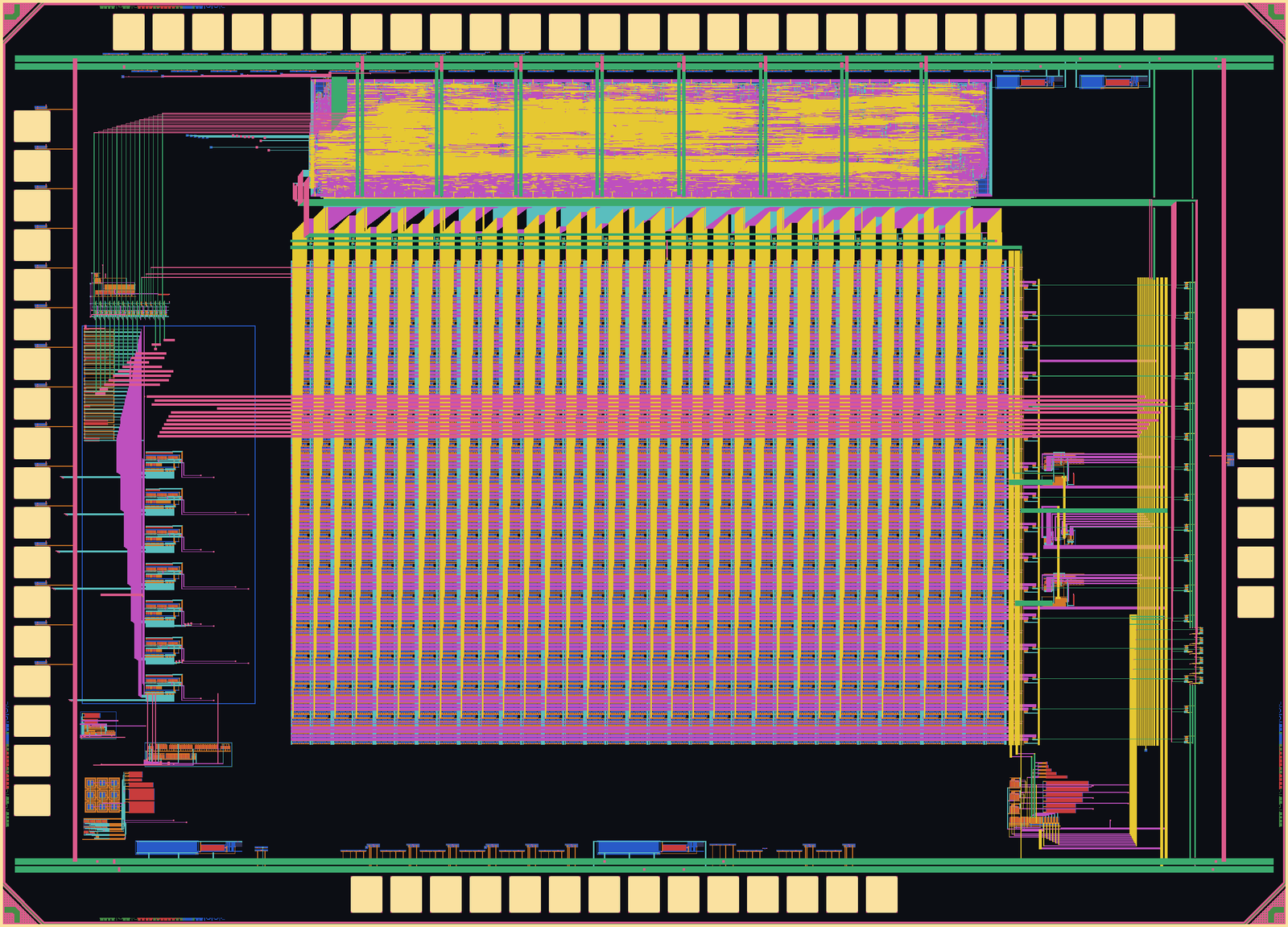
Floorplan
The analog tile and the digital core were designed as separate blocks and assembled at the top level. Placement principles:
- Column-interleaved P/N array: the two planes are not stacked but interleaved column by column (physical column 2p = Pj, 2p+1 = Nj). All banks share one orientation (matching), P/N are neighbours (differential), one SL net per plane.
- SL star node: the source lines of both planes reach the conveyor strip by the shortest path; SLP/SLN M4 row rails plus 10 µm M5 trunks on the right edge.
- Matching inside a bank: the six legs are common-centroid; the VBIAS gate line is distributed along the row in metal.
- Noise chain kept away from the array's switching noise, guard-ringed; short injection lines.
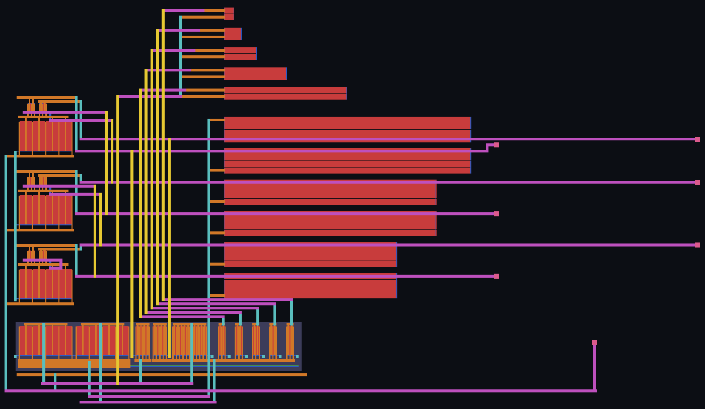
- Reference corner: bandgap PNPs (1:8 common-centroid), a single serpentine poly string (391 µm), trim multiplexers adjacent.
- Power domains: AVDD 2.5 V, VDD 1.2 V, AVDD_REF 2.5 V, VWL 1.0 V; four separate meshes, star connection on the board.
| Block | Size (µm) | Contents |
|---|---|---|
| ppu_tile (analog tile) | ≈ 1773 × 1212 | 544 synapse banks, row multiplexers, conveyors, fold, comparator, noise chain |
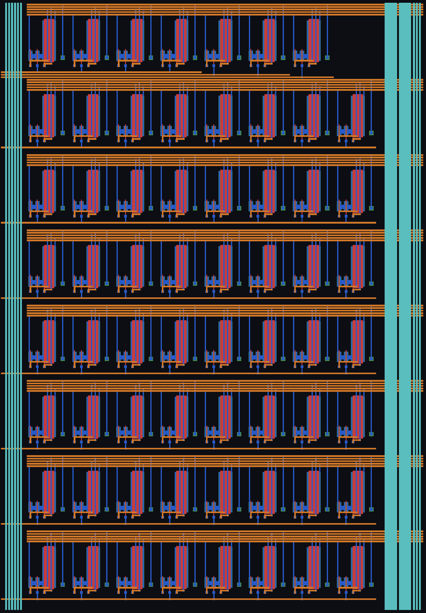
| ppu_synapse6 (bank) | 42.5 × 61.05 | 63 unit legs (6 binary-weighted groups), SL/BL M3 spines 1.2 µm (EM) |
| ppu_noise_therm2 | ≈ 248 × 144 | 3 gain stages + steerer; ≈ 800 µm of poly resistor |
| ppu_bandgap | ≈ 223 × 142 | PNP 1:8 common-centroid, start-up, 0.927 V reference |
| ppu_ref_rails | ≈ 353 × 768 | 391 µm poly string, 7 trim multiplexers, 7 buffers |
| ppu_vg_conveyor | ≈ 191 × 115 | Current conveyor holding SL at 0.150 V (×2) |
| ppu_fold_sa | ≈ 66 × 36 | Fold mirrors + StrongARM comparator |
| ppu_digital_top | ≈ 1378 × 244 | Synthesised digital core (SPI, register file, sequencer, spin register, weight latches) |
| ppu_pad_ring | 2600 × 1800 | 67 pads, ESD diodes, 4 power clamps, corner cells |
Analog blocks
Each block was rendered from its own GDS file. The colours follow the layer palette above.
Digital core

Verification (sign-off) results
All runs were made on the delivered geometry. DRC and density were run on the filled database, LVS and antenna on the unfilled one (the fill is floating and electrically inert).
| Check | Result | Date |
|---|---|---|
| DRC (full chip, filled) | 1728 rules / 0 violations | 26 Aug 2026 |
| Density (OD, PO, M1–M9, AP; 89 rules) | 0 violations | 26 Aug 2026 |
| LVS (full chip) | CORRECT — port names read from the pad labels | 26 Aug 2026 |
| Antenna (37 rules) | 0 violations (re-run on 27 Aug against the 26 Aug geometry, identical) | 27 Aug 2026 |
| Wire-bond rules | 0 violations | 26 Aug 2026 |
| ERC | 2 findings → waiver requests (below) | 26 Aug 2026 |
| Static timing — setup (WC / BC) | WNS +4.063 / +6.993 ns, TNS 0, ±5 % OCV derate | 26 Aug 2026 |
| Static timing — hold | WNS −22 ps, 131 endpoints → waiver request | 26 Aug 2026 |
| Dynamic IR drop (real gate-level VCD) | 30.9 mV = 3.4 %, 0 violations (no intentional on-chip decoupling) | 26 Aug 2026 |
Waiver requests to the foundry: three items only
| # | Item | Count | Nature |
|---|---|---|---|
| 1 | ERC "MOS connected to both power and ground" | 270 results / 540 geometries | By design: the ESD clamps across four supply domains |
| 2 | ERC floating N-well | 1 | By design. Went 55 → 36 → 1; two were real defects and were fixed |
| 3 | Hold WNS | −22 ps / 131 endpoints | With ±5 % derate; no functional risk |
DRC, LVS, antenna and wire-bond checks required no waivers.
Dummy fill: 6.25 million shapes
To satisfy the density rules, floating fill shapes connected to no net were added with an in-house generator to OD, PO, the nine metals and AP. The fill is entirely inside the die boundary. The filled database (chipfill.gds) is the submission candidate; the density rules are met only there.
All 89 density rules (OD, PO, M1–M9, AP; low and high limits) are clean on the filled database.
| Layer | GDS | Shapes | Edge (µm) |
|---|---|---|---|
| DOD (diffusion dummy) | 6;1 | 1 155 589 | 1.00 |
| DPO (poly dummy) | 17;1 | 1 164 918 | 0.80 |
| DUM1 … DUM7 | 31;1 … 37;1 | 3 478 537 | 1.20 |
| DUM8 | 38;1 | 336 893 | 1.60 |
| DUM9 | 39;1 | 106 819 | 3.00 |
| DAP (AP fill) | — | 1 816 | 20.00 |
| Total | 6 247 548 |