GDSII deliverables
The GDSII databases produced for tape-out, their top cells, label layers and the information declared in the delivery dossier. The GDSII files themselves are derived from the process design kit (PDK) and are not published here; their contents are documented below.
Two databases, one design
| File | Role | Top cell | Size | Structures | SHA-256 (first 16) | Date |
|---|---|---|---|---|---|---|
chipfill.gds | Submission candidate — the filled full chip. DRC and density were run on this file. | ppu65_chip_fill | 130 063 462 B | 318 | d012acf0ab56c8a0 | 26 Aug 2026 13:43 |
ppu65_chip.gds | Unfilled reference — the real macro merged with the seal ring. LVS and antenna were run on this file. | ppu65_chip | 80 608 670 B | 292 | 4fc7ca5e63c207ce | 26 Aug 2026 13:29 |
fill.gds | Dummy fill only (intermediate) | ppu_dummy_fill | — | — | — | 26 Aug 2026 |
Why two files? The dummy fill is floating (connected to no net) and electrically inert, so LVS and antenna checks are run on the unfilled version. The density rules are met only in the filled version, which is the one to be delivered. The SHA-256 of both files is recorded in the delivery document.
GDSII generation flow
The layout hierarchy is preserved: 292 structures in the unfilled file, 318 in the filled one; the difference is the 26-structure dummy-fill subtree. The fill lies entirely inside the die boundary (dummy bounding box −564.4 … 1984.9 × −344.85 … 1474.45 µm).
Label layers
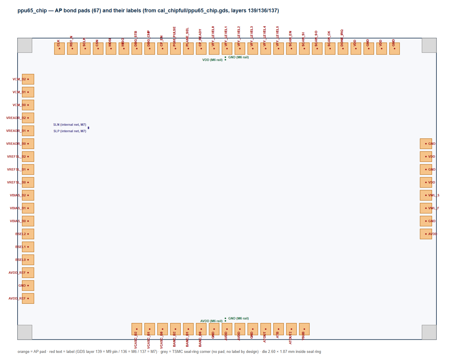
The pad labels are kept with the label purpose in the source database and stream out as pin-layer texts in the GDSII. 73 labels in total:
| GDS layer | Meaning | Labels | Content |
|---|---|---|---|
| 139 / 0 | M9 pin | 67 | The name of every bond pad; stick font, 6 µm |
| 136 / 0 | M6 pin | 4 | GND / VDD / AVDD power-rail labels, 8 µm |
| 137 / 0 | M7 pin | 2 | The tile's SLP / SLN internal nets (for LVS matching) |
To see the labels in a GDS viewer, layers 139/0, 136/0 and 137/0 must be visible and "show texts" enabled. At full-die zoom a 6 µm text is sub-pixel; it appears when zooming into a pad.
Example coordinates (pad centre, µm): CLK (−330, 1435) · MOSI (−10, 1435) · VCM_B2 (−525, 1245) · BSEL0 (−525, 125) · BANC_B0 (550, −305) · VSUB (1190, −305).
Block GDS files
Each analog block went through DRC/LVS separately with its own GDS and was then merged at the top level. The layout images on this site were rendered from these files.
| GDS | Top cell | Size (µm) | File | Note |
|---|---|---|---|---|
ppu65_chip.gds | ppu65_chip | 2600 × 1870 | 80.6 MB | full chip, unfilled |
ppu_tile.gds | ppu_tile | ≈ 1773 × 1212 | 10.7 MB | analog tile |
ppu_digital_top.gds | ppu_digital_top | ≈ 1378 × 244 | 48.9 MB | digital core (standard cells) |
ppu_pad_ring.gds | ppu_pad_ring | 2600 × 1800 | 6.4 MB | 67 pads + ESD |
ppu_synapse6.gds | ppu_synapse6 | 42.5 × 61.05 | 147 KB | synapse bank, 63 units |
ppu_noise_therm2.gds | ppu_noise_therm2 | ≈ 248 × 144 | 788 KB | thermal-noise chain v1.3 |
ppu_bandgap.gds | ppu_bandgap | ≈ 223 × 142 | 793 KB | bandgap reference |
ppu_vg_conveyor.gds | ppu_vg_conveyor | ≈ 191 × 115 | — | current conveyor |
ppu_fold_sa.gds | ppu_fold_sa | ≈ 66 × 36 | 201 KB | fold + StrongARM |
ppu_comp_latch.gds | ppu_comp_latch | ≈ 14 × 13 | 16 KB | comparator latch |
Deviations declared up front in the delivery dossier
- The GDSII contains 40 top-level structures. One is the real top cell (ppu65_chip_fill); the other 39 are unplaced via master cells referenced by nothing and contributing no mask geometry. If a single-top-cell file is required, a pruned version is ready: 279 structures, geometry-identical (278 of 279 structures byte-identical; the only difference is the top cell's timestamp).
- The polyimide (PM) layer is intentionally empty. Its acceptability for the selected package/assembly flow is to be confirmed by the foundry.
- LVS and antenna were run on the unfilled database, DRC and density on the filled one. The dummy fill is floating and electrically inert.
- No scan chain. Test access is through the SPI register interface and the 16-channel analog test mux.
- No intentional on-chip decoupling capacitance. Vector-based dynamic rail analysis: worst drop 30.9 mV = 3.4 %, 0 violations.
Backup: the delivery GDSII is not kept under version control (PDK derivative). A second copy is held in a compressed archive verified by SHA-256; moving that archive to external, encrypted storage is on the open-item list.